|
CB2 micro
Building guide
|

| Component
Label (on schematic) |
Component
Value |
Info/Markings/Codes
onto component |
Component
Photo |
Soldered
component photo |
Soldered? |
| - |
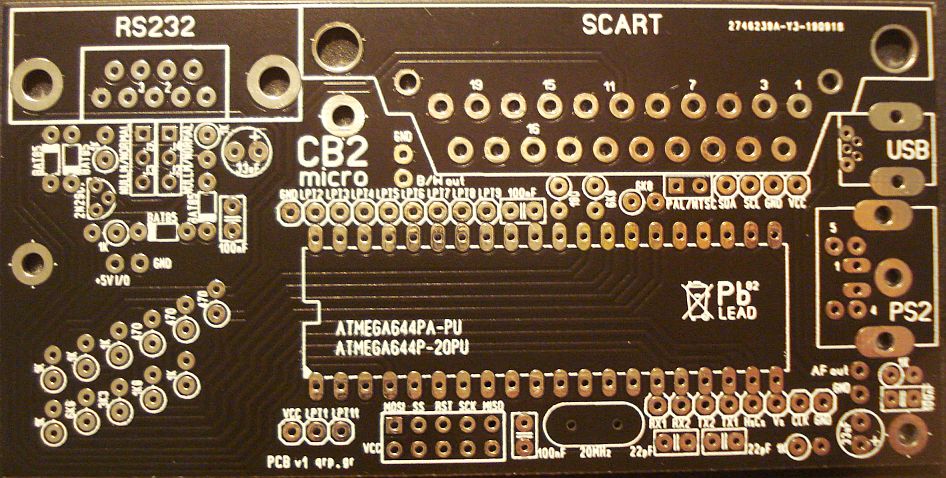
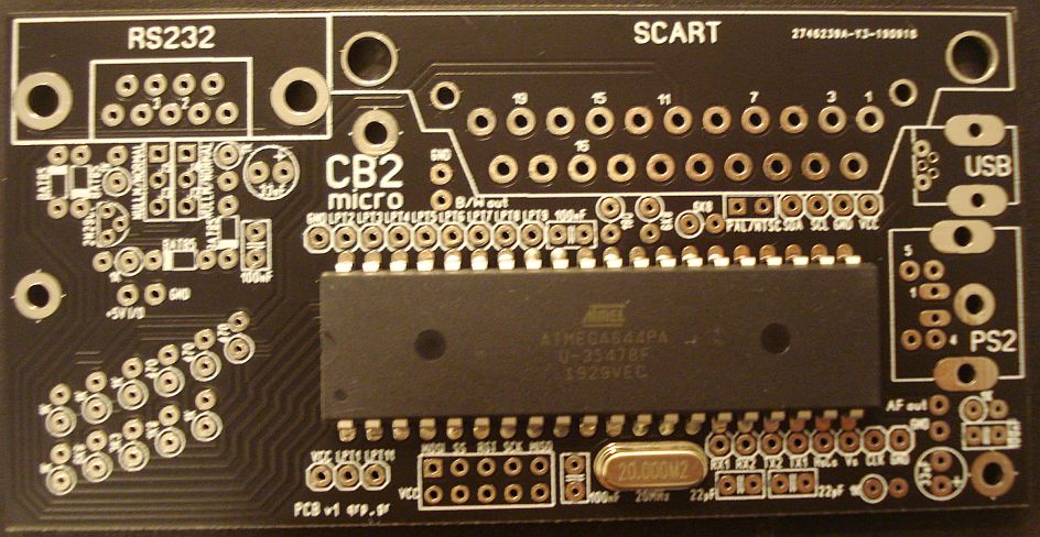
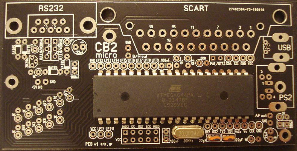
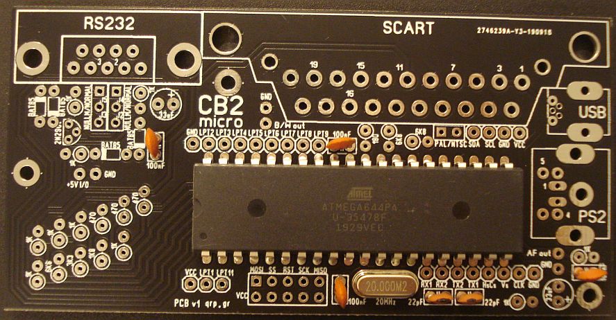
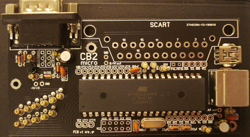
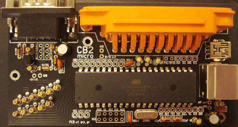
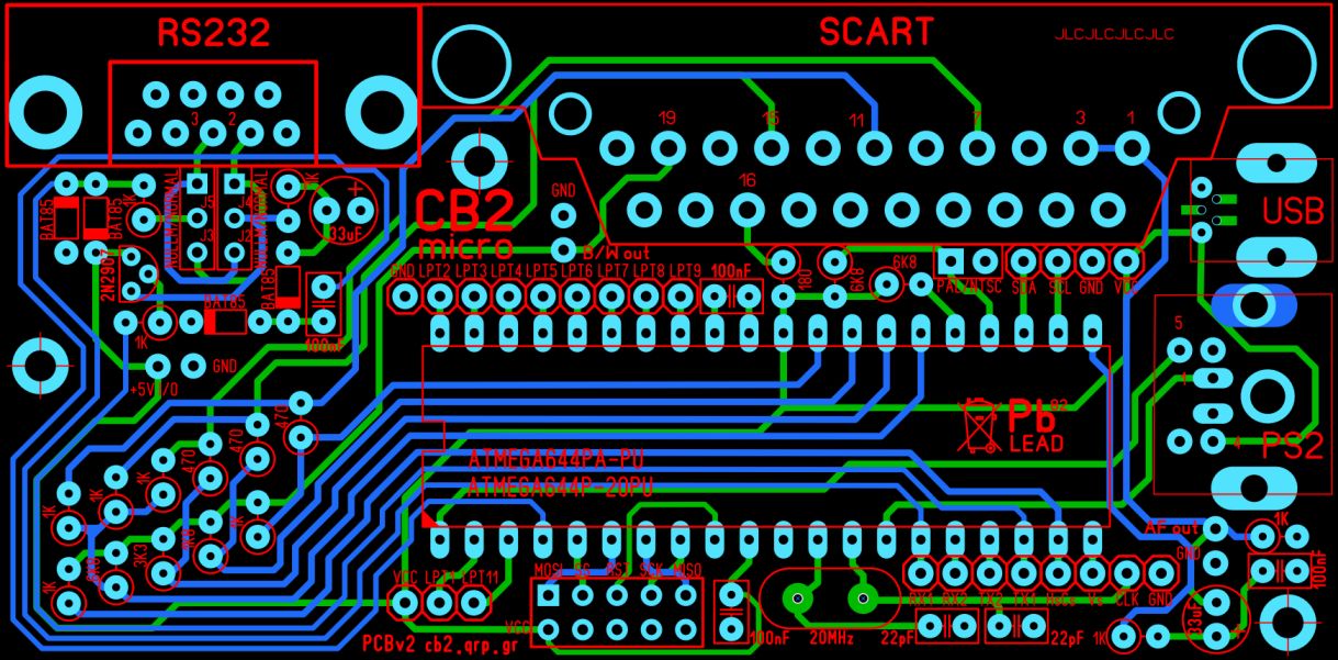
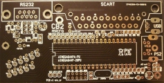
CB2 micro PCB |
CB2 micro * Note, since 2023, some purple PCBs are also available. |
 |
- |
- |
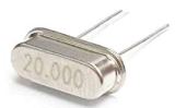
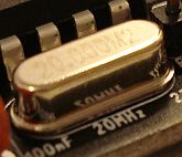
| X1 |
20MHz |
20.000 |
 |
 |
|
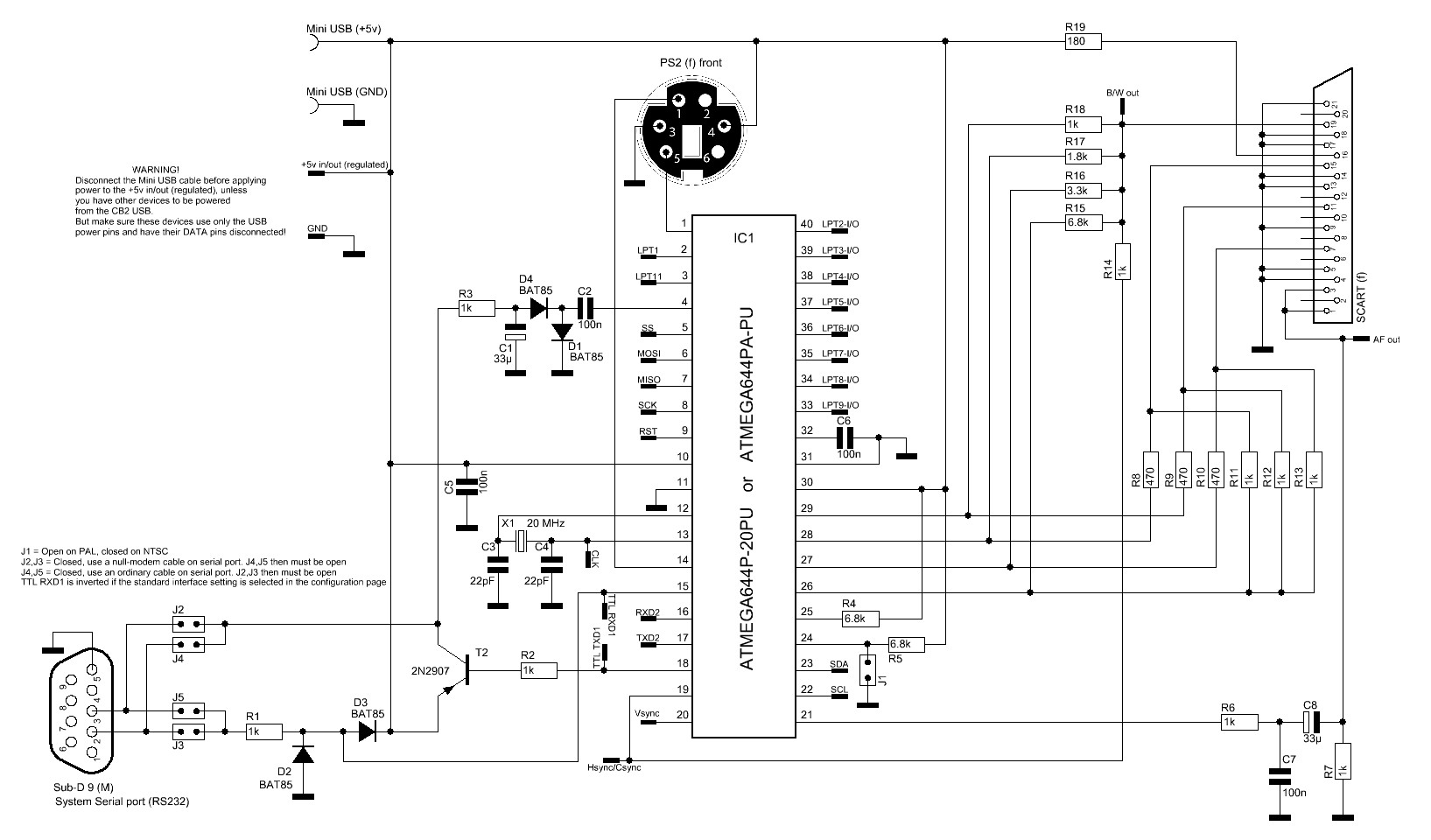
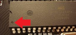
| IC1 | ATMEGA644P | ATMEGA644P-20PU or ATMEGA644PA-PU | 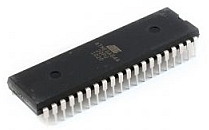 |
 |
|
| C3 | 22pF |
22 |
 |
 |
|
| C4 |
22pF |
22 |
|
|
|
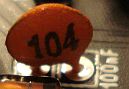
| C2 |
100nF | 104 |
 |
 |
|
| C5 |
100nF | 104 |
|
|
|
| C6 |
100nF | 104 |
|
|
|
| C7 |
100nF | 104 |
|
|
|
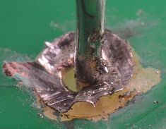
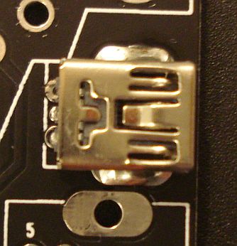
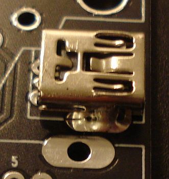
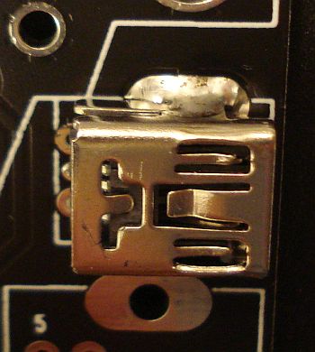
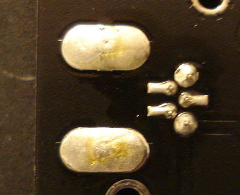
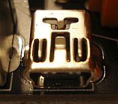
| Mini USB |
Mini USB connector |
Small metal connector * Note, since 2022, the connector comes mounted on the PCB, but you have to solder its pins. |
 |
 |
|
| D1 |
BAT85 |
BAT85 | 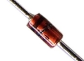 |
 |
|
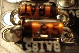
| D2 |
BAT85 | BAT85 | |
|
|
| D3 |
BAT85 | BAT85 | |
|
|
| D4 |
BAT85 | BAT85 | |
|
|
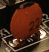
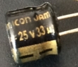
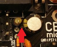
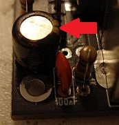
| C1 |
33uF |
33uF * Note, since 2022, the capacitor provided is longer. |
 |
 |
|
| C8 |
33uF |
33uF * Note, since 2022, the capacitor provided is longer. |
|
 |
|
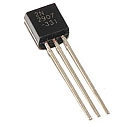
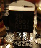
| T2 |
2N2907 |
2N2907 |
 |
 |
|
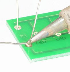
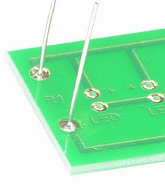
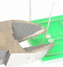
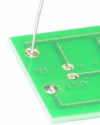
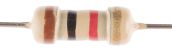
| R1 |
1k |
brown, black, red, gold * Note, since 2022, a blue resistor is supplied. |
 |
 |
|
| R2 |
1k |
brown, black, red, gold * Note, since 2022, a blue resistor is supplied. |
|
|
|
| R3 |
1k |
brown, black, red, gold * Note, since 2022, a blue resistor is supplied. |
|
|
|
| R6 |
1k |
brown, black, red, gold * Note, since 2022, a blue resistor is supplied. |
|
|
|
| R7 |
1k |
brown, black, red, gold * Note, since 2022, a blue resistor is supplied. |
|
|
|
| R11 |
1k |
brown, black, red, gold * Note, since 2022, a blue resistor is supplied. |
|
|
|
| R12 |
1k |
brown, black, red, gold * Note, since 2022, a blue resistor is supplied. |
|
|
|
| R13 |
1k |
brown, black, red, gold * Note, since 2022, a blue resistor is supplied. |
|
|
|
| R14 |
1k |
brown, black, red, gold * Note, since 2022, a blue resistor is supplied. |
|
|
|
| R18 |
1k |
brown, black, red, gold * Note, since 2022, a blue resistor is supplied. |
|
|
|
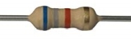
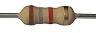
| R4 |
6.8k |
blue, gray, red, gold |
 |
|
|
| R5 |
6.8k |
blue, gray, red, gold |
|
|
|
| R15 |
6.8k |
blue, gray, red, gold |
|
|
|
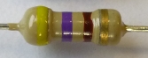
| R8 |
470 ohm |
yellow, violet, brown, gold |
 |
|
|
| R9 |
470 ohm |
yellow, violet, brown, gold |
|
|
|
| R10 |
470 ohm |
yellow, violet, brown, gold |
|
|
|
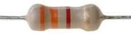
| R16 |
3.3k |
orange, orange, red, gold |
 |
|
|
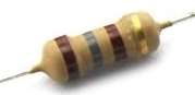
| R17 |
1.8k |
brown, gray, red, gold |
 |
|
|
| R19 |
180 ohm |
brown, gray, brown, gold |
 |
|
|
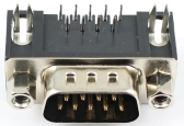
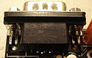
| Sub-D 9 (f) |
Dsub-9 male connector |
Big black plastic-metal connector |
 |
 |
|
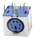
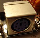
| PS2 (f) front |
PS/2 female connector |
Big metal connector. * Note, since 2022, a black connector is supplied. |
 |
 |
|
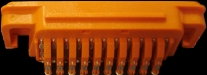
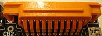
| SCART (f) |
SCART female connector |
Big plastic connector. * Note, since 10 Mar 2023, a black connector is supplied. |
 |
 |